Emerging Electronics
Solid State Electronics, Department of
Engineering Sciences, Uppsala University
Contact: Prof. Shili Zhang
www.teknik.uu.se/fte
This group focuses on electronic and optoelectronic devices based on nanostructures and functional materials. The research covers a broad spectrum from materials design, synthesis and analysis to device design, fabrication and characterisation. Principal process technologies are silicon technology, thin film technology and printing technology, where the group is strongly dependent on the facilities for processing and characterisation provided by MSL and the other Myfab laboratories. The group also contributes to the MSL services by providing expertise competence, primarily in printing technology. Research projects can be divided into the two main areas described below:
Flexible Electronics
This field targets a broad range of applications where mechanical flexibility and rollability are required, thus calling for low temperature, environment friendly fabrication on inexpensive and flexible plastic and polymeric substrates. Current research activities cover
• Development of solution-phase processing technology of carbon nanotubes and composites with functional polymers.
• Chemical vapour deposition for the growth of graphene primarily for flexible electronic applications.
• Area-selective surface functionalisation for pattern generation on plastic substrates and inkjet printing process for the fabrication of plastic electronic devices.
• Development and fundamentals of thin-film transistors based on carbon nanotubes and composites.
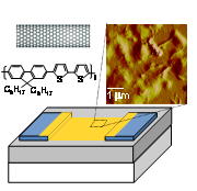
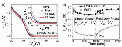
A thin-film transistor with solution-processed composite of carbon nanotubes and semiconducting polymer as the semiconductor channel (left), the transistor shows remarkably enhanced air stability (middle) and operational stability (right).
Nanostructures for Sensing
The mature silicon technology is combined with emerging electronic materials to develop various solutions in sensing and energy applications. Utilised nanostructures include nanoscale silicon strips, metal silicide films and carbon nanotubes. The research projects include
• Electrical field-effect biosensing using transistors with silicon nanowires and carbon nanotubes as the conduction channel.
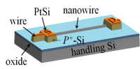
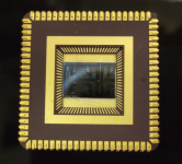
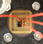
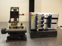
From left: Schematic of a silicon nanowire transistor (SiNWFET) fabricated using standard silicon technology; top-view picture of a bonded chip with SiNWFET arrays for simultaneous multiple sensing; top-view picture of the chip integrated with a microfluidic system with three inlets and one outlet all in orange tubing; photo picture of the measurement setup integrated with a syringe pump for bioassay delivery.
• Metal silicide films of tuneable thickness for energy applications.
Epitaxially aligned NiSi2 films grown on a Si(100) substrate with predetermined Ni incorporation.